91精品欧美激情在线播放-91精选视频在线观看-91九色成人-91九色在线视频-美女扒尿口给男人桶到爽-美女把尿口扒开让男人桶出水

Contact us
Send E-MAIL
Home ? Product Center ? Other ? Bare Die/Wafer ? LM5025A Die ?
A wafer, also called a slice or substrate, is a thin slice of semiconductor material, such as a crystalline silicon, used in electronics for the fabrication of integrated circuits and in photovoltaics for conventional, wafer-based solar cells. The wafer serves as the substrate for microelectronic devices built in and over the wafer and undergoes many microfabrication process steps such as doping or ion implantation, etching, deposition of various materials, and photolithographic patterning. Finally the individual microcircuits are separated (dicing) and packaged.


LM5025A Die 

 
Active Clamp Voltage Mode PWM Controller  

DIE/WAFER CHARACTERISTICS
Fabrication Attributes General Die Information
 Physical Die
 Identification
 LM5025A  Bond Pad Opening   Size  (min)  91μm x 91μm
 Die Step  A  Bond Pad Metalization  Al_ 0.5%Cu
Physical Attributes  Passivation  PECVDOX+NITRIDE
 Wafer Diameter  150mm  Back Side Metal  BARE BACK
 Die Size (Drawn)  2286μm x 2540μm         90.0mils x 100.0mils  Back Side Connection  Floating
 Thickness  254μm Nominal  
 Min Pitch  167μm Nominal  
Special Assembly Requirements:
Note: Actual die size is rounded to the nearest micron.
 
    LM5025 MDC MWC
    ACTIVE CLAMP VOLTAGE MODE PWM CONTROLLER
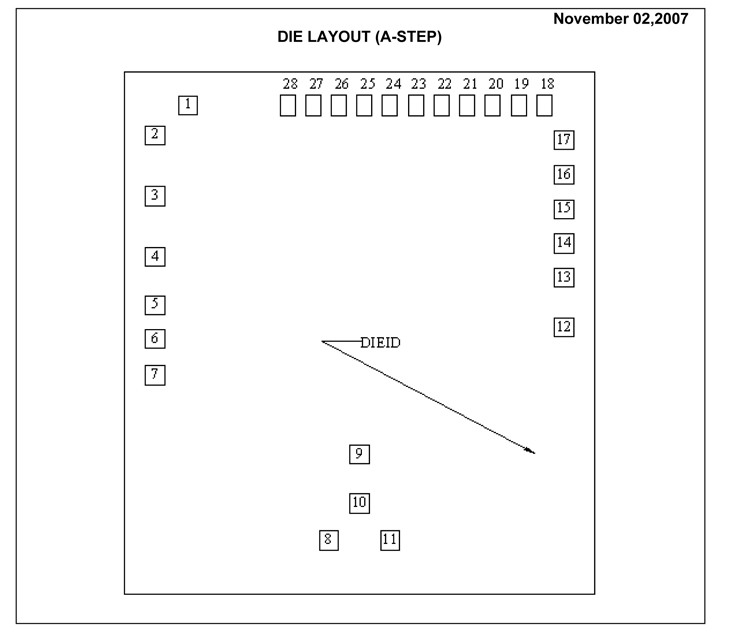
                          LM5025A Die封裝圖


Open
主站蜘蛛池模板: 房山区| 九龙城区| 渭源县| 万安县| 花莲市| 漯河市| 高密市| 广水市| 阿瓦提县| 金山区| 神农架林区| 永寿县| 高雄市| 阜城县| 鄂托克旗| 辉县市| 从江县| 留坝县| 油尖旺区| 闸北区| 宁陕县| 化州市| 绥中县| 嘉善县| 蓝田县| 治县。| 唐海县| 和田市| 耿马| 资溪县| 喀什市| 沛县| 吴旗县| 六枝特区| 潼关县| 玉树县| 沙坪坝区| 吴忠市| 江门市| 星子县| 平湖市|